PCIe Introduction
概述
本文主要介绍如下内容:
- PCIe的发展历程
- PCIe的Lane的概念介绍
- PCIe的1x,2x,4x,8x,16x Lane 引脚进行说明
简介
计算机硬件之间的通信分为两大类:
- 计算机内的通信
- 计算机间的通信
计算机内通信:
- 共享内存
- PCIe: CPU与GPU之间通信
- NVLink: GPU与GPU之间通信
计算机间通信:
- TCP/IP网络协议
- RDMA网络协议
其中 PCIe 是用于CPU与高速外设之间的通信总线, 像与以太网卡、固态硬盘,以及GPU等之间的通信。
PCIe, 是 Peripheral Component InterConnect Express 的缩写,是一种高速串行计算机扩展总线标准。主要用于扩展计算机系统总线数据吞吐以及提供设备通信速度。
PCIe 发展历程
| PCIe Version | Encoding | 传输速率 | 吞吐量 | Signaling | ||||
| x1 | x2 | x4 | x8 | x16 | ||||
| 1.0 | 8b/10b | 2.5 GT/s | 250 MB/s | 500 MB/s | 1 GB/s | 2 GB/s | 4 GB/s | NRZ |
| 2.0 | 8b/10b | 5 GT/s | 500 MB/s | 1 GB/s | 2 GB/s | 4 GB/s | 8 GB/s | NRZ |
| 3.0 | 128b/130b | 8 GT/s | 984.6 MB/s | 1.969 GB/s | 3.938 GB/s | 7.877 GB/s | 15.754 GB/s | NRZ |
| 4.0 | 128b/130b | 16 GT/s | 1.969 GB/s | 3.938 GB/s | 7.877 GB/s | 15.754 GB/s | 31.508 MB/s | NRZ |
| 5.0 | 128b/130b | 32 or 25 GT/s | 3.9 or 3.08 GB/s | 7.8 or 6.16 GB/s | 15.8 or 12.3 GB/s | 31.5 or 24.6 GB/s | 63 or 49.2 GB/s | NRZ |
| 6.0 | 128b/130b? | 64 GT/s | 16 GB/s | 32 GB/s | 64 GB/s | 128 GB/s | 256 GB/s | PAM4 |
| 7.0 | 128b/130b? | 128 GT/s | 32 GB/s | 64 GB/s | 128 GB/s | 256 GB/s | 512 GB/s | PAM4 |
PCIe 引脚说明
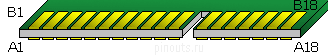
PCIe 1x Lane Connector 引脚
1x Lane 接口示意图如下图所示
其中每一引脚的含义如下表中所示
| Pin | Side B Connector | Side A Connector | ||
| 引脚编号 | 名称 | 描述 | 名称 | 描述 |
| 1 | +12v | +12 volt power | PRSNT#1 | Hot Plug Presence Detect |
| 2 | +12v | +12 volt power | +12v | +12 volt power |
| 3 | +12v | +12 volt power | +12v | +12 volt power |
| 4 | GND | Ground | GND | Ground |
| 5 | SMCLK | SMBus clock | JTAG2 | TCK |
| 6 | SMDAT | SMBus data | JTAG3 | TDI |
| 7 | GND | Ground | JTAG4 | TDO |
| 8 | +3.3v | +3.3 Volt power | JTAG5 | TMS |
| 9 | JTAG1 | +TRST# | +3.3v | +3.3 volt power |
| 10 | 3.3Vaux | 3.3v volt power | +3.3v | +3.3 volt power |
| 11 | WAKE# | Link Reactivation | PERST# | PCI-Express Reset signal |
| Mechanical Key | ||||
| 12 | RSVD | Reserved | GND | Ground |
| 13 | GND | Ground | REFCLK+ | Reference Clock, Differential pair |
| 14 | HSOp(0) | Transmitter Lane 0, Differential pair | REFCLK- | |
| 15 | HSOn(0) | GND | Ground | |
| 16 | GND | Ground | HSIp(0) | Receiver Lane 0, Differential pair |
| 17 | PRSNT#2 | Hotplug detect | HSIn(0) | |
| 18 | GND | Ground | GND | Ground |
PCIe 4x Lane Connector 引脚
4x Lane 接口示意图如下图所示
其中每一引脚的含义如下表中所示
| Pin | Side B Connector | Side A Connector | ||
| 引脚编号 | 名称 | 描述 | 名称 | 描述 |
| 1 | +12v | +12 volt power | PRSNT#1 | Hot Plug Presence Detect |
| 2 | +12v | +12 volt power | +12v | +12 volt power |
| 3 | +12v | +12 volt power | +12v | +12 volt power |
| 4 | GND | Ground | GND | Ground |
| 5 | SMCLK | SMBus clock | JTAG2 | TCK |
| 6 | SMDAT | SMBus data | JTAG3 | TDI |
| 7 | GND | Ground | JTAG4 | TDO |
| 8 | +3.3v | +3.3 Volt power | JTAG5 | TMS |
| 9 | JTAG1 | +TRST# | +3.3v | +3.3 volt power |
| 10 | 3.3Vaux | 3.3v volt power | +3.3v | +3.3 volt power |
| 11 | WAKE# | Link Reactivation | PERST# | PCI-Express Reset signal |
| Mechanical Key | ||||
| 12 | RSVD | Reserved | GND | Ground |
| 13 | GND | Ground | REFCLK+ | Reference Clock, Differential pair |
| 14 | HSOp(0) | Transmitter Lane 0, Differential pair | REFCLK- | |
| 15 | HSOn(0) | GND | Ground | |
| 16 | GND | Ground | HSIp(0) | Receiver Lane 0, Differential pair |
| 17 | PRSNT#2 | Hotplug detect | HSIn(0) | |
| 18 | GND | Ground | GND | Ground |
| 19 | HSOp(1) | Transmitter Lane 1, Differential pair | RSVD | Reserved |
| 20 | HSOn(1) | GND | Ground | |
| 21 | GND | Ground | HSIp(1) | Receiver Lane 1, Differential pair |
| 22 | GND | Ground | HSIn(1) | |
| 23 | HSOp(2) | Transmitter Lane 2, Differential pair | GND | Ground |
| 24 | HSOn(2) | GND | Ground | |
| 25 | GND | Ground | HSIp(2) | Receiver Lane 2, Differential pair |
| 26 | GND | Ground | HSIn(2) | |
| 27 | HSOp(3) | Transmitter Lane 3, Differential pair | GND | Ground |
| 28 | HSOn(3) | GND | Ground | |
| 29 | GND | Ground | HSIp(3) | Receiver Lane 3, Differential pair |
| 30 | RSVD | Reserved | HSIn(3) | |
| 31 | PRSNT#2 | Hot plug detect | GND | Ground |
| 32 | GND | Ground | RSVD | Reserved |
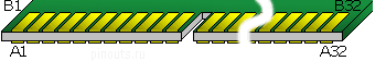
PCIe 8x Lane Connector 引脚
8x Lane 接口示意图如下图所示

其中每一引脚的含义如下表中所示
| Pin | Side B Connector | Side A Connector | ||
| 引脚编号 | 名称 | 描述 | 名称 | 描述 |
| 1 | +12v | +12 volt power | PRSNT#1 | Hot Plug Presence Detect |
| 2 | +12v | +12 volt power | +12v | +12 volt power |
| 3 | +12v | +12 volt power | +12v | +12 volt power |
| 4 | GND | Ground | GND | Ground |
| 5 | SMCLK | SMBus clock | JTAG2 | TCK |
| 6 | SMDAT | SMBus data | JTAG3 | TDI |
| 7 | GND | Ground | JTAG4 | TDO |
| 8 | +3.3v | +3.3 Volt power | JTAG5 | TMS |
| 9 | JTAG1 | +TRST# | +3.3v | +3.3 volt power |
| 10 | 3.3Vaux | 3.3v volt power | +3.3v | +3.3 volt power |
| 11 | WAKE# | Link Reactivation | PERST# | PCI-Express Reset signal |
| Mechanical Key | ||||
| 12 | RSVD | Reserved | GND | Ground |
| 13 | GND | Ground | REFCLK+ | Reference Clock, Differential pair |
| 14 | HSOp(0) | Transmitter Lane 0, Differential pair | REFCLK- | |
| 15 | HSOn(0) | GND | Ground | |
| 16 | GND | Ground | HSIp(0) | Receiver Lane 0, Differential pair |
| 17 | PRSNT#2 | Hotplug detect | HSIn(0) | |
| 18 | GND | Ground | GND | Ground |
| 19 | HSOp(1) | Transmitter Lane 1, Differential pair | RSVD | Reserved |
| 20 | HSOn(1) | GND | Ground | |
| 21 | GND | Ground | HSIp(1) | Receiver Lane 1, Differential pair |
| 22 | GND | Ground | HSIn(1) | |
| 23 | HSOp(2) | Transmitter Lane 2, Differential pair | GND | Ground |
| 24 | HSOn(2) | GND | Ground | |
| 25 | GND | Ground | HSIp(2) | Receiver Lane 2, Differential pair |
| 26 | GND | Ground | HSIn(2) | |
| 27 | HSOp(3) | Transmitter Lane 3, Differential pair | GND | Ground |
| 28 | HSOn(3) | GND | Ground | |
| 29 | GND | Ground | HSIp(3) | Receiver Lane 3, Differential pair |
| 30 | RSVD | Reserved | HSIn(3) | |
| 31 | PRSNT#2 | Hot plug detect | GND | Ground |
| 32 | GND | Ground | RSVD | Reserved |
| 33 | HSOp(4) | Transmitter Lane 4, Differential pair | RSVD | Reserved |
| 34 | HSOn(4) | GND | Ground | |
| 35 | GND | Ground | HSIp(4) | Receiver Lane 4, Differential pair |
| 36 | GND | Ground | HSIn(4) | |
| 37 | HSOp(5) | Transmitter Lane 5, Differential pair | GND | Ground |
| 38 | HSOn(5) | GND | Ground | |
| 39 | GND | Ground | HSIp(5) | Receiver Lane 5, Differential pair |
| 40 | GND | Ground | HSIn(5) | |
| 41 | HSOp(6) | Transmitter Lane 6, Differential pair | GND | Ground |
| 42 | HSOn(6) | GND | Ground | |
| 43 | GND | Ground | HSIp(6) | Receiver Lane 6, Differential pair |
| 44 | GND | Ground | HSIn(6) | |
| 45 | HSOp(7) | Transmitter Lane 7, Differential pair | GND | Ground |
| 46 | HSOn(7) | GND | Ground | |
| 47 | GND | Ground | HSIp(7) | Receiver Lane 7, Differential pair |
| 48 | PRSNT#2 | Hot plug detect | HSIn(7) | |
| 49 | GND | Ground | GND | Ground |
PCIe 16x Lane Connector 引脚
16x Lane 接口示意图如下图所示

其中每一引脚的含义如下表中所示
| Pin | Side B Connector | Side A Connector | ||
| 引脚编号 | 名称 | 描述 | 名称 | 描述 |
| 1 | +12v | +12 volt power | PRSNT#1 | Hot Plug Presence Detect |
| 2 | +12v | +12 volt power | +12v | +12 volt power |
| 3 | +12v | +12 volt power | +12v | +12 volt power |
| 4 | GND | Ground | GND | Ground |
| 5 | SMCLK | SMBus clock | JTAG2 | TCK |
| 6 | SMDAT | SMBus data | JTAG3 | TDI |
| 7 | GND | Ground | JTAG4 | TDO |
| 8 | +3.3v | +3.3 Volt power | JTAG5 | TMS |
| 9 | JTAG1 | +TRST# | +3.3v | +3.3 volt power |
| 10 | 3.3Vaux | 3.3v volt power | +3.3v | +3.3 volt power |
| 11 | WAKE# | Link Reactivation | PERST# | PCI-Express Reset signal |
| Mechanical Key | ||||
| 12 | RSVD | Reserved | GND | Ground |
| 13 | GND | Ground | REFCLK+ | Reference Clock, Differential pair |
| 14 | HSOp(0) | Transmitter Lane 0, Differential pair | REFCLK- | |
| 15 | HSOn(0) | GND | Ground | |
| 16 | GND | Ground | HSIp(0) | Receiver Lane 0, Differential pair |
| 17 | PRSNT#2 | Hotplug detect | HSIn(0) | |
| 18 | GND | Ground | GND | Ground |
| 19 | HSOp(1) | Transmitter Lane 1, Differential pair | RSVD | Reserved |
| 20 | HSOn(1) | GND | Ground | |
| 21 | GND | Ground | HSIp(1) | Receiver Lane 1, Differential pair |
| 22 | GND | Ground | HSIn(1) | |
| 23 | HSOp(2) | Transmitter Lane 2, Differential pair | GND | Ground |
| 24 | HSOn(2) | GND | Ground | |
| 25 | GND | Ground | HSIp(2) | Receiver Lane 2, Differential pair |
| 26 | GND | Ground | HSIn(2) | |
| 27 | HSOp(3) | Transmitter Lane 3, Differential pair | GND | Ground |
| 28 | HSOn(3) | GND | Ground | |
| 29 | GND | Ground | HSIp(3) | Receiver Lane 3, Differential pair |
| 30 | RSVD | Reserved | HSIn(3) | |
| 31 | PRSNT#2 | Hot plug detect | GND | Ground |
| 32 | GND | Ground | RSVD | Reserved |
| 33 | HSOp(4) | Transmitter Lane 4, Differential pair | RSVD | Reserved |
| 34 | HSOn(4) | GND | Ground | |
| 35 | GND | Ground | HSIp(4) | Receiver Lane 4, Differential pair |
| 36 | GND | Ground | HSIn(4) | |
| 37 | HSOp(5) | Transmitter Lane 5, Differential pair | GND | Ground |
| 38 | HSOn(5) | GND | Ground | |
| 39 | GND | Ground | HSIp(5) | Receiver Lane 5, Differential pair |
| 40 | GND | Ground | HSIn(5) | |
| 41 | HSOp(6) | Transmitter Lane 6, Differential pair | GND | Ground |
| 42 | HSOn(6) | GND | Ground | |
| 43 | GND | Ground | HSIp(6) | Receiver Lane 6, Differential pair |
| 44 | GND | Ground | HSIn(6) | |
| 45 | HSOp(7) | Transmitter Lane 7, Differential pair | GND | Ground |
| 46 | HSOn(7) | GND | Ground | |
| 47 | GND | Ground | HSIp(7) | Receiver Lane 7, Differential pair |
| 48 | PRSNT#2 | Hot plug detect | HSIn(7) | |
| 49 | GND | Ground | GND | Ground |
| 50 | HSOp(8) | Transmitter Lane 8, Differential pair | RSVD | Reserved |
| 51 | HSOn(8) | GND | Ground | |
| 52 | GND | Ground | HSIp(8) | Receiver Lane 8, Differential pair |
| 53 | GND | Ground | HSIn(8) | |
| 54 | HSOp(9) | Transmitter Lane 9, Differential pair | GND | Ground |
| 55 | HSOn(9) | GND | Ground | |
| 56 | GND | Ground | HSIp(9) | Receiver Lane 9, Differential pair |
| 57 | GND | Ground | HSIn(9) | |
| 58 | HSOp(10) | Transmitter Lane 10, Differential pair | GND | Ground |
| 59 | HSOn(10) | GND | Ground | |
| 60 | GND | Ground | HSIp(10) | Receiver Lane 10, Differential pair |
| 61 | GND | Ground | HSIn(10) | |
| 62 | HSOp(11) | Transmitter Lane 11, Differential pair | GND | Ground |
| 63 | HSOn(11) | GND | Ground | |
| 64 | GND | Ground | HSIp(11) | Receiver Lane 11, Differential pair |
| 65 | GND | Ground | HSIn(11) | |
| 66 | HSOp(12) | Transmitter Lane 12, Differential pair | GND | Ground |
| 67 | HSOn(12) | GND | Ground | |
| 68 | GND | Ground | HSIp(12) | Receiver Lane 12, Differential pair |
| 69 | GND | Ground | HSIn(12) | |
| 70 | HSOp(13) | Transmitter Lane 13, Differential pair | GND | Ground |
| 71 | HSOn(13) | GND | Ground | |
| 72 | GND | Ground | HSIp(13) | Receiver Lane 13, Differential pair |
| 73 | GND | Ground | HSIn(13) | |
| 74 | HSOp(14) | Transmitter Lane 14, Differential pair | GND | Ground |
| 75 | HSOn(14) | GND | Ground | |
| 76 | GND | Ground | HSIp(14) | Receiver Lane 14, Differential pair |
| 77 | GND | Ground | HSIn(14) | |
| 78 | HSOp(15) | Transmitter Lane 15, Differential pair | GND | Ground |
| 79 | HSOn(15) | GND | Ground | |
| 80 | GND | Ground | HSIp(15) | Receiver Lane 15, Differential pair |
| 81 | PRSNT#2 | Hot plug present detect | HSIn(15) | |
| 82 | RSVD#2 | Hot Plug Detect | GND | Ground |